01/The Core Insight
The core insight
InP and GaN have long lacked an easy way to make lattice‑matched distributed Bragg mirrors (DBRs) with enough refractive‑index contrast for truly high reflectivity. InPHRED solves this by turning selected epitaxial layers into a nanoporous form, precisely tuning optical index—an effect reminiscent of nature’s nanostructural optics (butterfly wings, ultra‑white beetles, Pollia fruit). The result is a homoepitaxial “super‑mirror” DBR that can be grown using standard foundry MOCVD.
02/The Breakthrough
How we solved a 30-year deadlock
A long-standing industry barrier solved by a single, foundry-compatible process.
The industry has been stuck for 30 years
1
GaAs VCSELs dominate NIR (850–980 nm) because AlGaAs/GaAs forms a near-perfect homoepitaxial DBR mirror pair: high refractive-index contrast, mature process, wafer-level testable, low cost. These VCSELs are in every iPhone and LiDAR sensor today.
2
InP (SWIR) and GaN (visible) have no equivalent DBR pair. Lattice-matched InP alloys yield only ~0.3% index contrast versus ~16% for AlGaAs/GaAs, far below the ~99.9% mirror reflectivity required to sustain a VCSEL optical cavity. GaN faces the same fundamental barrier.
3
All workarounds fail to scale. Heteroepitaxial growth is expensive and defect-prone. Wafer fusion disrupts the monolithic process flow. Double dielectric DBRs require complex post-processing. No competitor has achieved low-cost, wafer-level InP or GaN VCSELs commercially.
InPHRED's patented nanoporous solution
✓
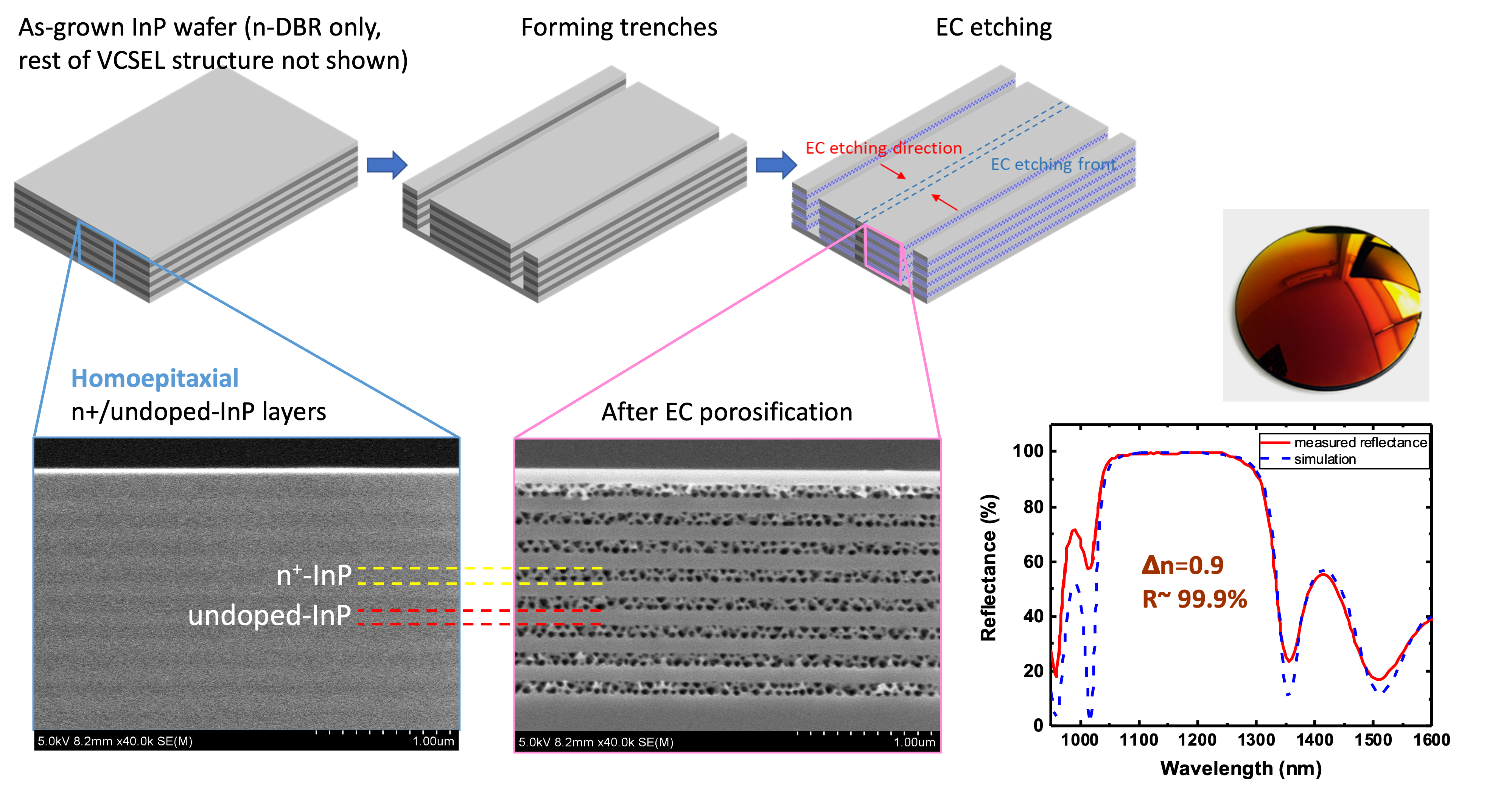
Electrochemical nanoporous etching selectively converts n⁺-doped semiconductor layers into nanoporous material — reducing local refractive index by a precisely controllable amount, determined entirely by porosity. Undoped layers remain unchanged.
✓
Homoepitaxial DBR with engineered index contrast. Alternating dense and nanoporous layers create refractive-index steps of up to ~40% (exceeding AlGaAs/GaAs contrast) on standard foundry-grown InP or GaN epi. No exotic materials or wafer fusion are required.
✓
Drop-in compatible with volume manufacturing. The porosification step is a single post-epi electrochemical process added to a conventional wafer-level flow. We leverage foundry fab and on-wafer testing compatible with the compound semiconductor supply chain.
03/Commercial Performance
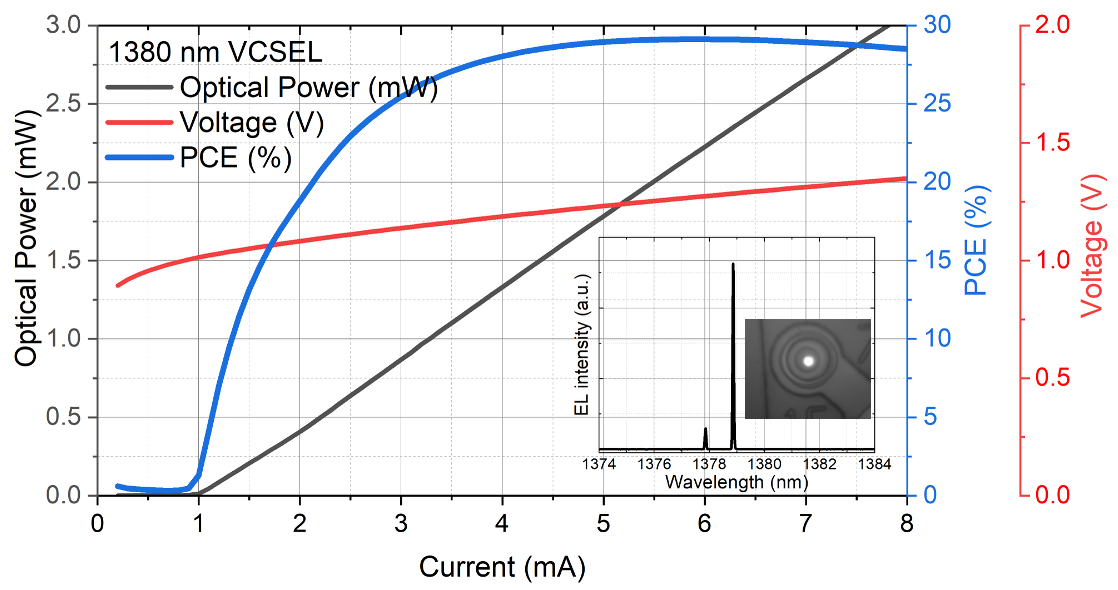
World's first mass-market SWIR VCSEL
Production-grade efficiency and single-mode lasing demonstrated on standard foundry-grown InP epi.
04/Competitive Landscape
No other technology meets the demand for low-cost manufacturability
Compared to all prior InP VCSEL approaches, InPHRED's homoepitaxial nanoporous DBR is uniquely manufacturable at commercial scale and low cost.
| Heteroepitaxial DBR Bandwidth10, RayCan |
AlAs/GaAs on GaAs IQE |
Wafer fusion BeamExpress, Trumpf |
Double dielectric DBR Vertilas |
InPHRED nanoporousOUR APPROACH | |
|---|---|---|---|---|---|
| DBR epitaxy | Difficult heteroepitaxy | Mature AlGaAs | Mature AlGaAs | N/A | Homoepitaxy, mature |
| Wavelength range | 1,300–1,600 nm | Up to 1,300 nm | 1,300–1,600 nm | 1,300–1,600 nm | 1,300–2,300 nm |
| Active region | ✓ Mature | ⚠ Reliability issues | ✓ Mature | ✓ Mature | ✓ Mature |
| Monolithic fab | Wafer-level | Wafer-level | ✗ Not scalable | ✗ Not scalable | Wafer-level |
| Volume production | ✗ Difficult | ⚠ Marginal | ✗ Difficult | ✗ Difficult | ✓ Excellent |
| Cost | Medium | Medium | High | High | Low |
05/Intellectual Property
A deepening IP moat
Our exclusive license covers the core nanoporous DBR process, application to specific material systems and device geometries, and downstream integration approaches. The portfolio grows with every new application we develop.
Discuss licensing or partnerships →- Core porosification process: electrochemical conversion of n⁺-doped InP and GaN layers to nanoporous semiconductor with controlled porosity and index contrast
- InP VCSEL DBR architecture: nanoporous/dense InP layer pairs forming a homoepitaxial Bragg reflector for SWIR lasing (1,300–2,300 nm)
- GaN RC-LED for wearables: nanoporous GaN DBR mirrors bounding a visible-light resonant cavity for high-spectral-purity emission (450–570 nm)
- Additional patentable technologies: 2–4 further patentable innovations developed since our seed round, covering advanced device and process variations